
Integrated Quantum Photonics
Figures for scientific publications
During the last years I have had the honor to create multiple figures for publications of the Integrated Quantum Photonics Group at Humboldt-Universität zu Berlin led by Prof. Tim Schröder.
Below are examples of my work for the group, with figure captions from the publications and links to the full papers.
Quantum electrometer for time-resolved material science at the atomic lattice scale
Working principle of the quantum electrometer
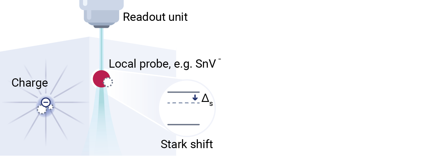
The local probe is an optically-active atomic defect with non-linear Stark-sensitive energy-levels. The read-out unit is a photoluminescence excitation spectroscopy microscope.
Charge dynamics in diamond
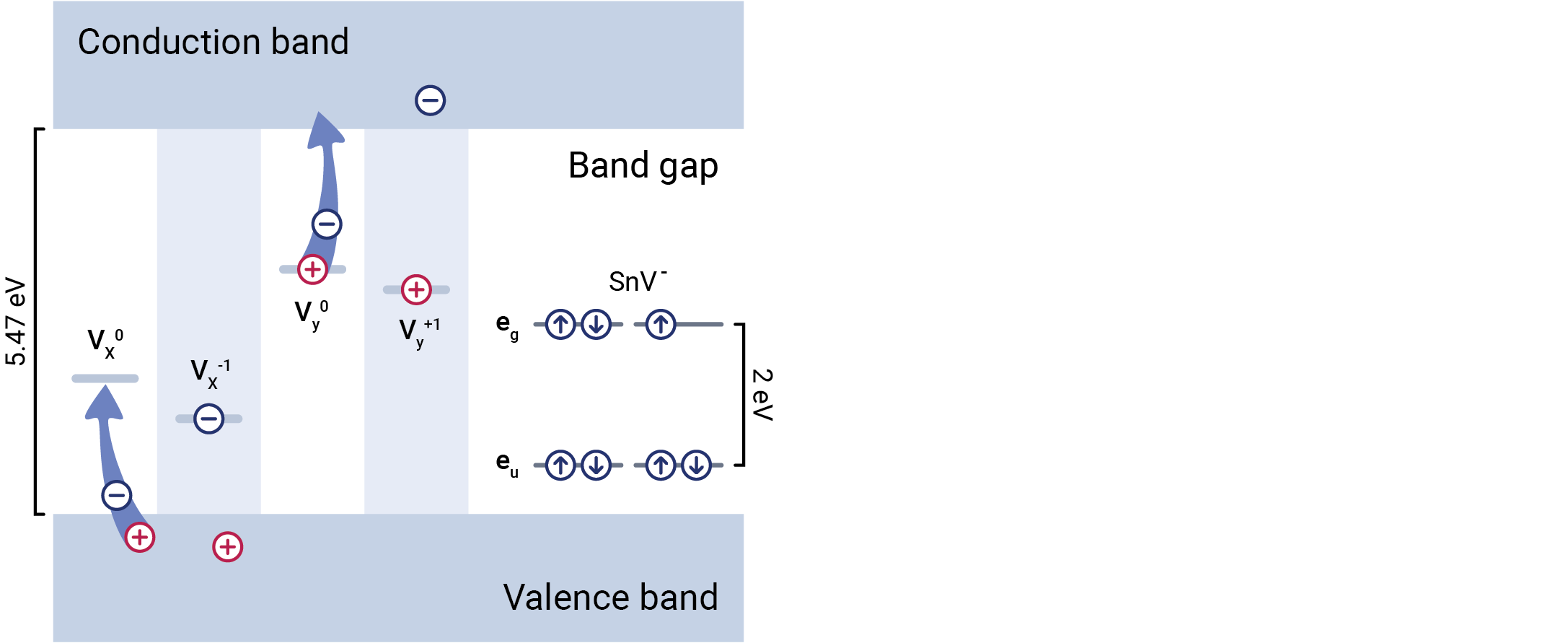
Illustration of an SnV, ionized and neutral defects (Vx,y) in the diamond bandgap. Ionization occurs when either an electron is promoted from the valence band to the charge trap, or an electron is promoted from the trap to the conduction band by an illumination field. Neutralization occurs when the trap either catches a hole from the valence band or an electron from the conduction band.
Divacancy (V2) creation during annealing
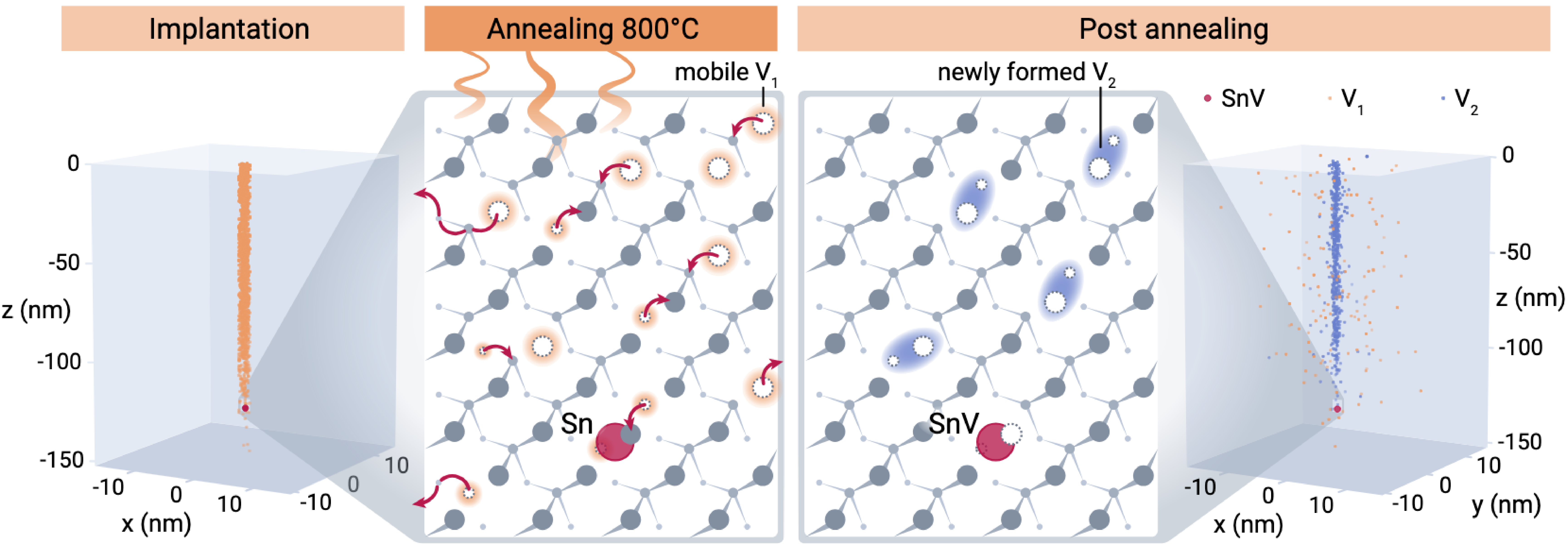
Implantation panel: Spatial distribution of created monovacancies (V1) by 400 keV Sn implantation predicted by SRIM simulations.
Annealing panel: V2 formation during annealing at 800 ◦C. At elevated temperatures, V1 start diffusing. Then, V1 immobilize either by moving to the boundaries, recombining with interstitial carbons, or forming V2.
Post annealing panel: Distribution of V1 and V2 which are distributed in the vicinity of the damage channel caused by the Sn implantation.
Zoom in: V2 in the vicinity of the SnV.
Full paper: Quantum electrometer for time-resolved material science at the atomic lattice scale Gregor Pieplow, Cem Güney Torun, Charlotta Gurr, Joseph H. D. Munns, Franziska Marie Herrmann, Andreas Thies, Tommaso Pregnolato, and Tim Schröder; Nature Communications volume 16, Article number: 6435 (2025)
Optically Coherent Nitrogen-Vacancy Defect Centers in Diamond Nanostructures
Schematic sketch of a NV incorporated in a nanopillar
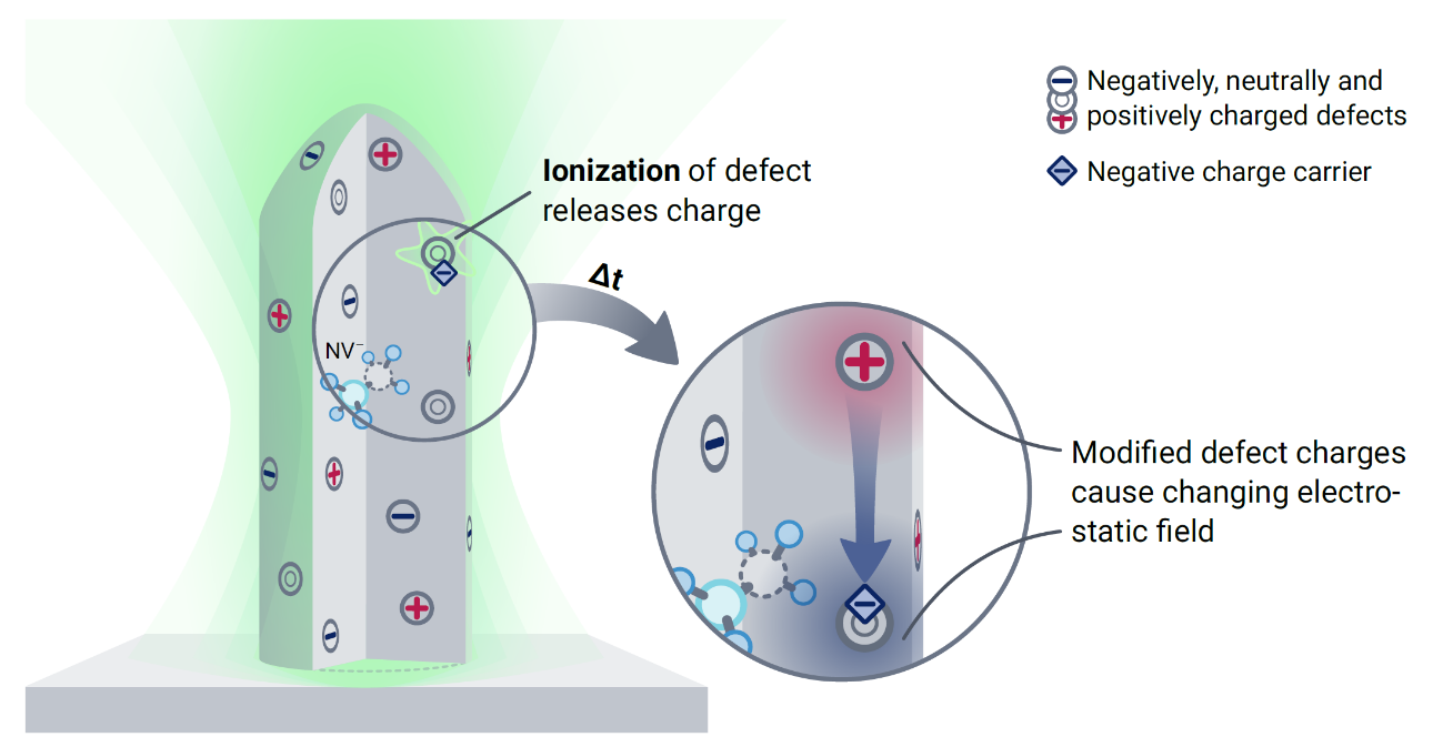
Green laser irradiation causes ionization of present surface and bulk defects; i.e., charges are released and move within the lattice, for example, to other defects that act as charge traps. This dynamic induces fluctuations of the electrostatic environment of the NV and leads to spectral diffusion of the NV ZPL.
Full paper: Optically Coherent Nitrogen-Vacancy Defect Centers in Diamond Nanostructures
Laura Orphal-Kobin, Kilian Unterguggenberger, Tommaso Pregnolato, Natalia Kemf, Mathias Matalla, Ralph-Stephan Unger, Ina Ostermay, Gregor Pieplow, and Tim Schröder; Phys. Rev. X 13, 011042 – Published 20 March 2023
Diamond-on-chip infrared absorption magnetic field camera
Working principle of the chip-integrated NV-based multi-pixel magnetic field camera.
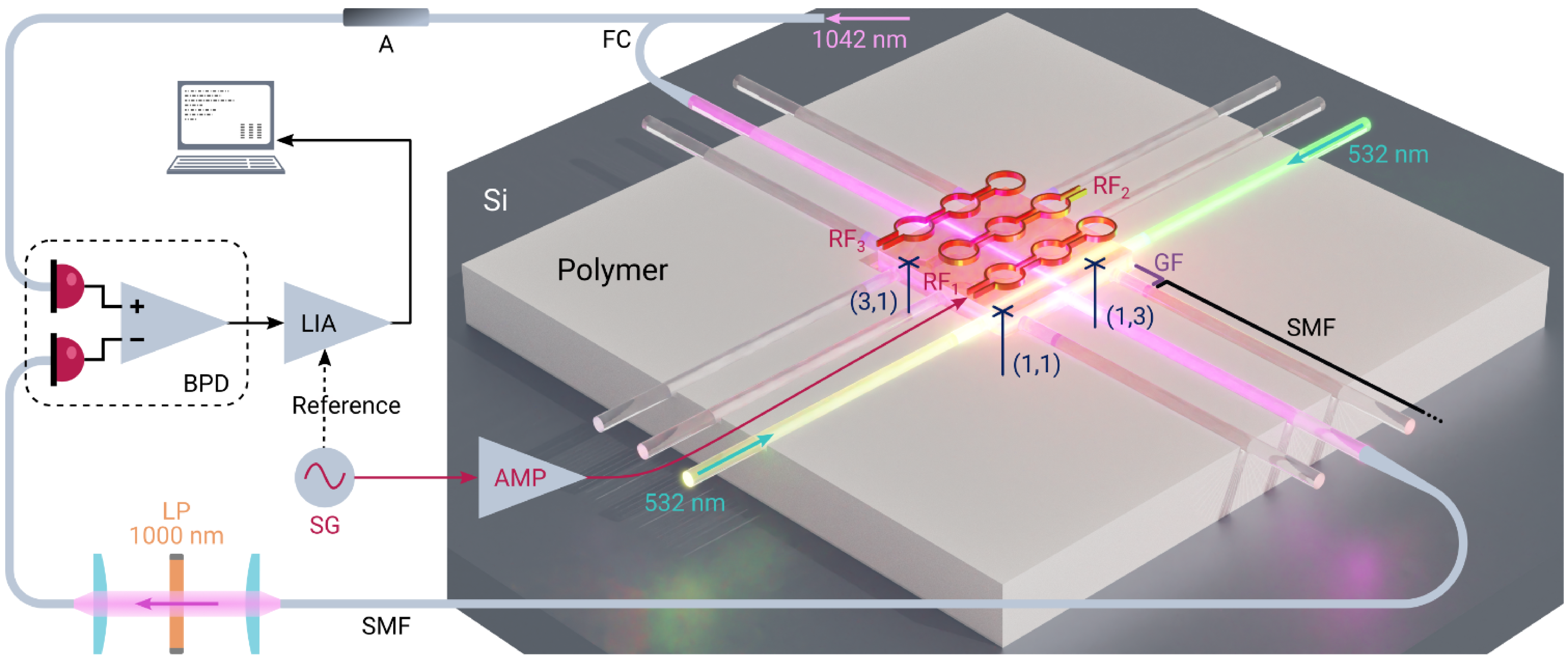
A diamond substrate and single-mode fibers (SMF) terminated by beam-collimating graded-index fibers (GF) are glued into trenches etched into a polymer substrate. The polymer covers a silicon submount (Si) for stability. Intersecting 532 nm pump and 1042 nm infrared laser beams define the magnetic sensitive pixel (i, j) inside the diamond substrate. 10 % of the injected infrared light is split off by a fiber coupler (FC) and directed to the reference input of a balanced photodetector (BPD) after passing an adjustable fiber attenuator (A). The infrared light transmitted through the diamond substrate passes a 1000 nm longpass filter (LP) located in a fiber U-bench before it reaches the BPD’s signal input. The BPD’s difference signal is amplified by a lock-in amplifier (LIA) and processed with a computer. A signal generator (SG) provides a reference for the LIA-demodulation and generates a frequency-modulated microwave signal which is amplified (AMP) and fed into the respective microwave inductor line (RFi) located above the row of active (pumped) pixels.
The chip rendering was provided by the IQP team and I designed the schematic of the working principle around it.
Full paper: Diamond-on-chip infrared absorption magnetic field camera
Julian M. Bopp, Hauke Conradi, Felipe Perona, Anil Palaci, Jonas Wollenberg, Thomas Flisgen, Armin Liero, Heike Christopher, Norbert Keil, Wolfgang Knolle and others; arXiv preprint arXiv:2401.00854 (2023)